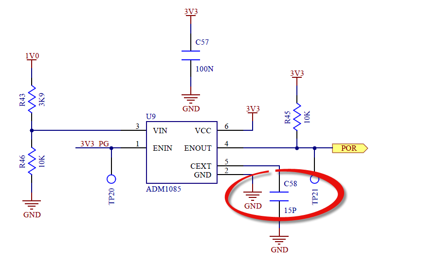
Latest schematic is uploaded.
The Programmer's interface buffer window has two tabs, one for data (code memo), and another for viewing the part's config and status registers (config). Prior to programming the flash I enable QE in this register. See attached image.
Thanks,
Dan
XHRA-2HPA No USB Activity Topic is solved
-
DHembree
- Experienced Member
- Posts: 75
- Joined: Fri Apr 15, 2016 6:46 pm
You do not have the required permissions to view the files attached to this post.
View Solution
-
mon2

- XCore Legend
- Posts: 1913
- Joined: Thu Jun 10, 2010 11:43 am
Dan, some comments:
1) Review the use of a DC-DC convertor that can consolidate the power good feature into a single package:
http://www.rohm.com/web/global/products ... BD9A100MUV
http://www.digikey.com/product-detail/e ... ND/4878924
Then you can remove U13 from the circuit.
2) Another thought is to source a 1v0 version of the voltage supervisor for U8 and then again U13 can be removed for this single device.
On U8, allow for a CT cap in case the delay needs to be tweaked. Allow for adjustable voltage resistors in case the fixed threshold part is not available.
3) Pin 23 of the XMOS CPU must always mate to Vbus of the USB connector.
4) Will you use USB Type B connector or Micro USB ?
5) Details of X1 ? Assuming 3v3 SMD oscillator. Should be < $0.30 USD in single T&R qty. Not using the usual Si5351A PLL as per ref designs ?
6) R6-R9 could be consolidated into a single resistor network (0603x4 = 1206 footprint) to save on assembly costs (ie. single placement covers 4 parts)
7) R1, R3, R5 could be consolidated into a single resistor network (0603x4 = 1206 footprint) to save on assembly costs.
8) R11 & R12 could be consolidated into a single resistor network (0603x4 = 1206 footprint) to save on assembly costs.
9) There are lower cost and better ESD protection devices than D4 (TI).
Better options are:
SOCAY p/n ULC0524P
http://www.socay.com/upfile/201407020248027678.pdf
* suitable for USB 2.0 and USB 3.1 Gen 1 (aka USB 3.0)
* ultra low capacitance
$0.042 USD in 3k T&R qty (MOQ), Shenzhen, CN.
(same footprint) as Littlefuse p/n SP3012-04
http://www.mouser.com/ProductDetail/Lit ... 52bg%3D%3D
To further enhance the designs, insert some current limit circuit or device into Vbus. Polymer fuses (< $ 0.20 USD from Digikey) are common here but they do derate after numerous triggers. A more robust and faster reaction time but more expensive can be found in solid state USB load switches which offer reverse current protection and also selectable current triggers. Review the many public Arduino designs for ideas on USB current protection using polymer SMD fuses.
Example of a suitable polymer fuse for USB projects:
http://www.digikey.com/product-detail/e ... ND/4156209
10) What are the details of L1 ? We have used Taiyo Yuden in the past with success:
http://www.digikey.com/product-detail/e ... ND/1008284
11) U10 may be replaced with a 200 mA (Max) LDO from Toshiba as a cost reduction (please confirm if the 200mA is suitable for the 3v3 rail)
TCR2EF33,LM(CT
http://www.digikey.com/product-detail/e ... CR2EF33,LM(CT/TCR2EF33LM(CTTR-ND/4503183
12) What are the details of S1? Recommend that the switch is sealed so the PCB assembly can be machine washable.
-
mon2

- XCore Legend
- Posts: 1913
- Joined: Thu Jun 10, 2010 11:43 am
XMOS is listing a 15pf cap for the power on reset delay with the ADM1085 in the XCORE-200 Explorer Kit schematics.
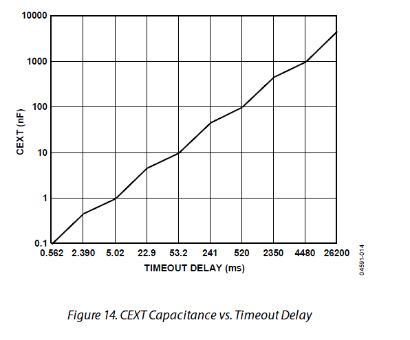
When comparing to the Analog datasheet, Figure 14, believe that this value is in error in the XMOS XCORE-200 schematic. Perhaps should be marked as 15nf for C58 ? Otherwise, 15pf = 0.015nF which does not look to be correct.


When comparing to the Analog datasheet, Figure 14, believe that this value is in error in the XMOS XCORE-200 schematic. Perhaps should be marked as 15nf for C58 ? Otherwise, 15pf = 0.015nF which does not look to be correct.


-
DHembree
- Experienced Member
- Posts: 75
- Joined: Fri Apr 15, 2016 6:46 pm
Mon2
I appreciate all of your suggestions, and while they are all excellent points on reducing system costs, this particular board is merely a proof-of-concept design, so cost reduction is not of primary concern. I am really just after functionality at this point. I will take them into consideration moving forward, particularly power scheme ideas.
I am finished implementing the design changes and am going to send the board to fab. I was wondering if you had addressed the "golden" flash request?
The value of the ADM1085 reset timing capacitor on my design is 2.2nF. I agree that the value in the XCORE-200 schematic seems erroneous.
Thanks,
Dan
-
mon2

- XCore Legend
- Posts: 1913
- Joined: Thu Jun 10, 2010 11:43 am
Hi Dan. About to work on a few ideas to clone the original XMOS supplied flash. Have assorted 8 pin SOIC devices in the building now. Also have initiated a few variations of programming tools to offer the public in the near future (varying in costs and features).
Let me supply more feedback after some testing of the flash clone but hope to have a working model soon. Digging for some XMOS tools which are MIA at this time of writing.
Let me supply more feedback after some testing of the flash clone but hope to have a working model soon. Digging for some XMOS tools which are MIA at this time of writing.
-
mon2

- XCore Legend
- Posts: 1913
- Joined: Thu Jun 10, 2010 11:43 am
Dan, can you post a dump of your QSPI flash that you are using ? Do not believe there is anything sacred inside the flash device so should be safe for public viewing. Otherwise you can email to me directly: kumar[at]softio.com.
Wish to compare your binary image against the original and likewise, if your image as-is (with QSPI bit enabled) will function on our original XMOS ref board.
Wish to compare your binary image against the original and likewise, if your image as-is (with QSPI bit enabled) will function on our original XMOS ref board.
Last edited by mon2 on Tue Nov 08, 2016 7:56 pm, edited 1 time in total.
-
DHembree
- Experienced Member
- Posts: 75
- Joined: Fri Apr 15, 2016 6:46 pm
I posted the image I am programming to flash a few messages back image_swap.bin, I believe. Is this what you are interested in?
Dan
Dan
-
mon2

- XCore Legend
- Posts: 1913
- Joined: Thu Jun 10, 2010 11:43 am
Dan - I see the jpg for your configuration / tool and the pdf but not the image at the top of this page. Please confirm. I think the bin file did not get posted.
-
DHembree
- Experienced Member
- Posts: 75
- Joined: Fri Apr 15, 2016 6:46 pm
Bin file types are not allowed. Must have missed that. Here it is inside a zip.
You do not have the required permissions to view the files attached to this post.
-
mon2

- XCore Legend
- Posts: 1913
- Joined: Thu Jun 10, 2010 11:43 am
Have it now. Thanks.
Bin file types are not allowed.
Did not know that :) Be back after a review.
Bin file types are not allowed.
Did not know that :) Be back after a review.
