So a PG signal is sent to the sequencer - it introduces a delay and then send the Power in Reset which we would want to tie together with the possible Reset when connected to the X-tag? And there would not be any other way to tie the RST lines unless I apply the buffer circuit?
Also about the sequencer. Why is it needed. It would only seem logical that you would like a delay after the core receives full 1V before putting the RST pin to 0, but I do not have a technical explanation for it. My other thought was the sequencer is just needed to produce a pulse as the RST should be constantly 0 during work, but to actually reset you would need a pulse to 1.
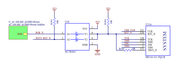
Review the exact truth table for part used in the design. The part will output a logic low while the input voltage is under the 1 volt level. Once the threshold is reached, the output will be high-z (open; high impedance). The external pull up resistor will soft pull up to a high level. The XMOS cpu will remain in reset state if the pin is LOW.
The outputs of these buffers are tied together so that the XTAG tool can also perform a reset at anytime. This is only possible as shown due to the open drain outputs.
Once the voltage level is met, there is a delay and then the buffer becomes open to release the cpu out of reset.

