Hi,
The datasheet on page 4 states that the device has "Up to 32 x 1bit port".
But chapter "4 Signal Description" writes only about 16 1bit ports. Than how many 1 bit ports this device has?
XL210-512-TQ128 number of 1bit ports Topic is solved
-
Endre
- Active Member
- Posts: 38
- Joined: Fri Jan 01, 2016 10:13 am
-
mon2

- XCore Legend
- Posts: 1913
- Joined: Thu Jun 10, 2010 11:43 am
See page 6 & 7 of the same datasheet and if you read the pin table from RIGHT to LEFT, you will see the priority of the port widths. That is, if you assign a large port width then the same smaller port width cannot be used in your software.
If the port width is greyed out then that port width is not complete but is available for your consideration. Take for example, the 32 bit width, it is in greyed out color in the datasheet, this implies that you can map the port block as a 32 bit port but do note that not all 32 port pins are bonded out.
Next, review the possible use of 16B0..16B15 on Tile # 0 (prefix X0) = all 16 bit port pins are available but note that these pins overlap with the single bit port widths. For this reason, if you do decide to use this block as a 16 bit port width then you may not use the same overlapping single port pins. Specifically, 1M0..1P0 cannot be used if you decide to use this region of port pins as a 16 bit port block. Again, the port width priority is from the RIGHT to LEFT assignment.
Respectively, page 6 and 7 define the single port widths of 1A0..1P0 and these are bonded to Tile # 0 (labeled as prefix of X0 for Tile #0).
Respectively, page 8 defines the single port widths of 1A0..1P0 and these are bonded to Tile # 1 (labeled as prefix of X1 for Tile #1).
It is important to have a solid understanding of these relationships else your code will tickle the incorrect port pins. One of the recommended learning tools is to try a simply blinky program with a local LED. Do the same for Tile # 0 and also Tile # 1, etc.
Some XMOS devices feature a single Tile while others have 2 or more Tiles. Inside each such Tile are logical CPU cores and the number of such logical CPU cores will vary with the hardware and also your software coding. To gain the highest throughput / speed, review each component's datasheet to understand the maximum MIPs possible if you proceed to use the recommended # of CPU cores.
Summary: There are indeed 16 single port pins on Tile # 0. Also, another 16 single port pins on Tile # 1.
Last edited by mon2 on Wed May 18, 2016 12:05 pm, edited 1 time in total.
-
Endre
- Active Member
- Posts: 38
- Joined: Fri Jan 01, 2016 10:13 am
Thanks!
Now it is getting clear for me,I guess.
So X0D00 can be configured as 1A0 which is driven by Tile0, and X1D00 can be also configured as 1A0, but that is driven by Tile1.
Now it is getting clear for me,I guess.
So X0D00 can be configured as 1A0 which is driven by Tile0, and X1D00 can be also configured as 1A0, but that is driven by Tile1.
-
mon2
- XCore Legend
- Posts: 1913
- Joined: Thu Jun 10, 2010 11:43 am
First, trust us to say that we have all had some struggle to understand this complex beast. It is a small learning curve but you are almost there.
So for your specific CPU,
X0D00 = Pin 32 on the TQFP package. This port pin can be assigned as P1A0 on Tile # 0.
X1D00 = Pin 84 on the TQFP package. This port pin can be assigned as P1A0 on Tile # 1.
In your software coding, you must reference the specific Tile # to tickle the proper port pin.
Here is an example of code that demands this style of reference:
http://www.xcore.com/forum/viewtopic.ph ... 35&p=22099
Since you are considering the XCORE-200 series, assuming you have the XCORE-200 Explorer Kit or similar ?
Note the nomenclature where for P1A0 ==> P1 = "single bit port". A0 = "reference this port pin as Bit #0 of Port A".
Often, there is some confusion with developers (including us) who are learning about XMOS on such relationships.
A small piece of advice is to also review the pricing for the assorted XMOS devices. You may be surprised that it may make more sense to purchase say another P/N which features perhaps USB and/or Ethernet but not use those functions. That is, sometimes, such parts are more readily available through Digikey or Future Electronics, etc. due to their popularity as compared to perhaps the exact P/N you are seeking. This will allow you to source a drop in replacement of the XMOS CPU often in single piece qty at very competitive costs.
Technically correct but please note that the 1A0 bonded to X0 tile is a physical different pin on the XMOS CPU as compared to the 1A0 bonded to the X1 tile. It will be best to review each and every datasheet for the CPU you plan to use. Do not stop reading as sometimes there are typos in the data sheet. Also does not hurt to ping back to this public user forum for advice from other developers (and XMOS employees who often chime in here) to be sure you have nailed it before creating a custom PCB, etc.So X0D00 can be configured as 1A0 which is driven by Tile0, and X1D00 can be also configured as 1A0, but that is driven by Tile1.
So for your specific CPU,
X0D00 = Pin 32 on the TQFP package. This port pin can be assigned as P1A0 on Tile # 0.
X1D00 = Pin 84 on the TQFP package. This port pin can be assigned as P1A0 on Tile # 1.
In your software coding, you must reference the specific Tile # to tickle the proper port pin.
Here is an example of code that demands this style of reference:
http://www.xcore.com/forum/viewtopic.ph ... 35&p=22099
Since you are considering the XCORE-200 series, assuming you have the XCORE-200 Explorer Kit or similar ?
Note the nomenclature where for P1A0 ==> P1 = "single bit port". A0 = "reference this port pin as Bit #0 of Port A".
Often, there is some confusion with developers (including us) who are learning about XMOS on such relationships.
A small piece of advice is to also review the pricing for the assorted XMOS devices. You may be surprised that it may make more sense to purchase say another P/N which features perhaps USB and/or Ethernet but not use those functions. That is, sometimes, such parts are more readily available through Digikey or Future Electronics, etc. due to their popularity as compared to perhaps the exact P/N you are seeking. This will allow you to source a drop in replacement of the XMOS CPU often in single piece qty at very competitive costs.
-
Dukuu
- Junior Member
- Posts: 4
- Joined: Thu May 19, 2016 1:52 pm
Hi! I've read the mon2 reply's, thanks a lot!
Looks like my search request on this forum really corresponds the answers from mon2 in this thread.
I am just newbie in xMOS processors, and quite possible i ask obvious things...
So. My puzzle is connected with ports and ethernet PHY on xCORE-200 explorer kit.
I have to port old project from L16 processor to xCORE-200 explorer kit. I found example of AN00199_-XMOS-Gigabit-Ethernet-application-note_1.0.1rc1 and checked it to work on the board. It works. I took old project to change ports and tiles to make it work on 200 processor. And that's where i was really puzzled. The port mapping differs a lot in old project and in example. My exploring the xCORE 200 manuals and code resulted in a table. Check it please:
1. AN00199 example (I took ports from code) uses much more ports than i can see in tables of ports in board's manual.
2. XE216-512-TQ128 Datasheet shows the table of signals, and next it shows the picture , where I can see the same signals, as in example...
3. but i go back to board manual, and all i see is , that enumerates less signals than used in example.
This is strange and i found no description for this at this time. Possibly I'll be pointed to the correct place to read? Or simple explanation can be read as an answer to this thread?
And the main question to mon2 is in . Look at orange and violet cells in table. The same port should do totally different routine work on different bits/pins. Can you explain that?
Here is the orange cells from that table:
4E2 8C6 rx2
4E3 8C7 rx3
4E0 8C0 tx_clk
4E1 8C1 tx_ctl
How different bits of the port can partly do input and partly do output?
Note, these ports does not have 1-bit ports under them.
Thanks in forward for any info, explanations or links that will show something clear.
You do not have the required permissions to view the files attached to this post.
-
mon2
- XCore Legend
- Posts: 1913
- Joined: Thu Jun 10, 2010 11:43 am
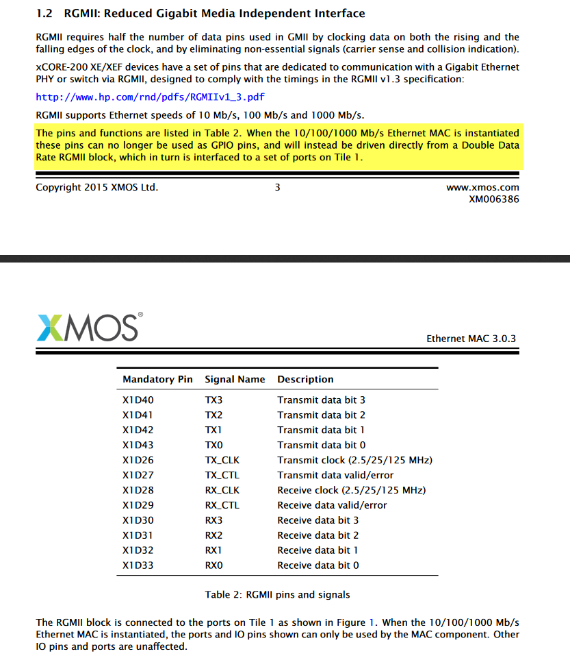
Hey Dukuu. To date, we have not had to be concerned about the same port pins. The following document (section 1.2) may explain it the best on what is going on inside the RGMII interface present on the XCORE-200 devices:
http://www.xmos.com/download/private/li ... .3rc1).pdf
* see pages 3 & 4
From our understanding this means that if you do enable the use of the Gigabit MAC (RGMII) interface then you will lose the functions of the related and overlapping port pins due to internal multiplexing of the same physical pins for this high speed interface. That is, you are no longer dealing with the standard 4 bit ports noted in the datasheet so the restrictions of same direction of data transfer no longer apply. While you are using the referenced port pins, you are not working with the 4B ports but rather dedicated hardware inside the chip to permit the RGMII interface to operate correctly. Same physical port pins on this package are being used by different internal pieces of hardware.
On this note, the XS1 designs bit bang like mad to interface with external hardware such as 10/100 Mbit ethernet PHYs, etc. for which the code is based on the use of high speed ports.
Perhaps someone from XMOS can confirm but that is our interpretation. Hope this helps.
-
Dukuu
- Junior Member
- Posts: 4
- Joined: Thu May 19, 2016 1:52 pm
mon2, thanks a lot! Sounds interesting. Is it a theory? Or this is how it works? I didn't read such a info anywhere until now.mon2 wrote:...you are no longer dealing with the standard 4 bit ports noted in the datasheet so the restrictions of same direction of data transfer no longer apply. While you are using the referenced port pins, you are not working with the 4B ports but rather dedicated hardware inside the chip to permit the RGMII interface to operate correctly. Same physical port pins on this package are being used by different internal pieces of hardware.
henk thanks to you, all you say is good. I understand the things, that are happening after external pins of the IC package. I do not understand the internal process.
So, as a conclusion from your posts:
if IC has an RGMI or other external phy, than inside the chip something changes in comparison with "standart" package, MUXes, or port-map or some port handler.
on the other side, I would think, that if IC had an ability to use some pins as 1-bit ports it would use it, and the PDF would show that. All other ports, that can work as 1+8+16 bit port are listed in pin-maps tables.
and the question is still here:
P4E0 tx_clk
P4E1 tx_ctl
P4F0 rx_clk
P4F1 rx_ctl
P4F2 rx0
P4F3 rx1
P4E2 rx2
P4E3 rx3
how should I initiate these ports, when they are available for me just as 4-bit ports, and they should be out and in at the same time?
-
henkVerified
- Respected Member
- Posts: 347
- Joined: Wed Jan 27, 2016 5:21 pm
mon2 is completely correct.
There are some devices that can be connected using one bit ports, such as:
- SPI boot flash
- QSPI boot flash
- USB PHY
- RGMII interface
You need one of the first two - and if you buy an F part it will be a QSPI boot flash embedded in the device
The latter two - you only loose the listed ports if you actually use the device
Finally the last one, if you want to use an RGMII PHY you must also connect them as shown to the X1Dxx pins.
About the tables - there are IO pins (XxDxx), there are ports (XS1_PORT_xx), there are links (XxLx), and there are special function IO devices (RGMII).
- The IO pins refer to the physical pins.
- The other three are muxed onto the IO pins, so it may be that the RGMII devices use the IO pins in one way, and the ports in a different way.
Also note that port 8D would use XxD36..43 as all inputs or all outputs, but that when you use port 1M..P they can each individually be in or out.
Hope this helps,
Henk
-
henkVerified
- Respected Member
- Posts: 347
- Joined: Wed Jan 27, 2016 5:21 pm
Hi Dukuu,
If you don't use RGMII - you can ignore all RGMII functions on the pins. Only when RGMII is enabled will the pins be used for RGMII, otherwise they will be used for GPIO as normal (i.e., there is a bus-switch inside the chip, it will connect the pins to either ports 4E and 4F, or to the RGMII workings).
Assuming your are not using RGMII:
port 4E on tile 1: you can use that as all inputs, or all outputs.
port 4F on tile 1: you can use that as all inputs, or all outputs.
(as with all other multi-bit ports, they are all in or all out).
Hope this helps,
Henk
-
Dukuu
- Junior Member
- Posts: 4
- Joined: Thu May 19, 2016 1:52 pm
Thanks all for answers, looks like i got the things.
In short - I'm now using the AN00199 example code, and penetrating into it my other tasks. That is not so optimal as could be but for my learning purposes - enough.
The XE216 pdf, that i re-read after got the answers in this topic, was found to say some vital thing in brackets:
In comparison with other project (on L16), that was given to me as an example, the XE216 chip has specialized block, that overrides the pins to communicate directly with RGMII PHY.
On L16 all the job was done via GPIO routine, as PHY was external, and it's Eth10/100 data transmission was made in software. This is particular difference, that i didn't got on the beginning, and stuck into it. Thanks for answers, hope others will get it easier.
In short - I'm now using the AN00199 example code, and penetrating into it my other tasks. That is not so optimal as could be but for my learning purposes - enough.
The XE216 pdf, that i re-read after got the answers in this topic, was found to say some vital thing in brackets:
I don't know (for now) how to activate RGMII via a register, but sure that it can be found in PDFs. So to use RGMII one should communicate with the register or use standard libraries.XE216-512-TQ128 Datasheet, page 20 wrote:When RGMII mode is
enabled (using processor status register 2) these pins can no longer be used as
GPIO pins, and will instead be driven directly from an RGMII block
In comparison with other project (on L16), that was given to me as an example, the XE216 chip has specialized block, that overrides the pins to communicate directly with RGMII PHY.
On L16 all the job was done via GPIO routine, as PHY was external, and it's Eth10/100 data transmission was made in software. This is particular difference, that i didn't got on the beginning, and stuck into it. Thanks for answers, hope others will get it easier.