Hi,
QE bit in QSPI flash is set properly.
I synchronize my scope with the falling edge of the SCK input to QSPI flash.
The second channel is connected to the ID0 line.
When I power up my board or EVB board, my scope (in single shot mode) catches the EBh command on both boards. I assume that this is the first command that is sent from XHRA to the QSPI flash. Clock frequencies are different: 2.5 MHz on EVB and 10 MHz on my board. On both boards, the input clock to XHRA is the same 24MHz and clock levels are the same.
I will investigate the reset signals in detailed way although we have nearly the same reset configuration as on the EVB.
Wlodek
XHRA QSPI flash booting problem
-
wlodek
- Member++
- Posts: 22
- Joined: Fri Jul 22, 2016 3:19 pm
-
wlodek
- Member++
- Posts: 22
- Joined: Fri Jul 22, 2016 3:19 pm
Hi again,
I have performed the followin checks:
- SI535A clock to XHRA = 24 MHz on both EVB and my board (levels the same)
- When XHRA starts on power up, the EBh command (fast read) is issued by XHRA to QSPI flash.
On the EVB the clock to QSPI flash is 2,5 MHz,
On my board the clock to QSPI flash is 10 MHz (??)
Next 3 bytes sent on I0..I3 are 0 (starting address) (on both EVB and my board+
Byte 4th is ? (I did not decode it on scope)
Then 4 clocks are meaningless.
Next come the data from the memory. I tried to decode it from my scope and it seems to start from D3h 70h.
This seems to be exactly what I have programmed at first two bytes in my QSPI flash.
I also checked that the CE# does not go HIGH on my board and the EBh (fast read) is working in never ending loop (what is probably normal behaviour of QSPI flash read command when CE# is LOW and clocks are provided).
When checking the EVB I noticed that after some 12 us the CE# goes HIGH for a while and then the next command is issued to the QSPI. (seems like XHRA requested some 16 bytes from QSPI flash with the firs read command).
Attached are screenshots from my scope.
Box_1_IO_2SCK.zip shows the power up on my board. Channel number 1 shows data from data line (I0 first picture, I3 last picture) and channel number 2 shows the clock. Sync was done with the rising edge of the clock signal.
EVB_1_IO_2SCK.zip shows the power up on XMOS Eval board. Channel number 1 shows data from data line (I0 first picture, I3 last picture) and channel number 2 shows the clock. Sync was done with the rising edge of the clock signal.
Note that time bases are different as I have different clock frequencies.
You do not have the required permissions to view the files attached to this post.
-
henkVerified
- Respected Member
- Posts: 347
- Joined: Wed Jan 27, 2016 5:21 pm
Would you be able to post some schematics?
I am happy to have a look at them to see if there is anything odd.
I am happy to have a look at them to see if there is anything odd.
-
mon2

- XCore Legend
- Posts: 1913
- Joined: Thu Jun 10, 2010 11:43 am
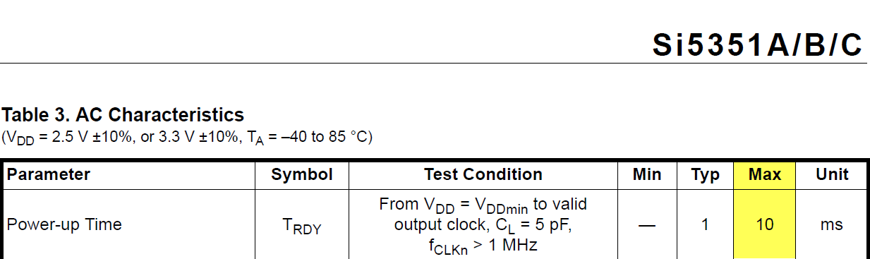
According to the Si5351A PLL datasheet, this PLL may take up to 10 ms to power up. Wondering if this could be an issue.
Have you tried to borrow the clock out from the working XMOS EVB and feed into your PCB to rule out the PLL as a root cause ?
Also try to (cleanly) pulse #RESET on the XMOS CPU to see if the QSPI clock changes or remains @ 10 Mhz.
Have you tried to borrow the clock out from the working XMOS EVB and feed into your PCB to rule out the PLL as a root cause ?
Also try to (cleanly) pulse #RESET on the XMOS CPU to see if the QSPI clock changes or remains @ 10 Mhz.
-
wlodek
- Member++
- Posts: 22
- Joined: Fri Jul 22, 2016 3:19 pm
Hi,
Attached find the schematics of audiobridge part of my board. The Reset to the XHRA had to be slightly modified to get 1 V only after 3.3 V goes to its level.
We also removed the TVS between QSPI memory and XHRA (we plan to use ISP flash in future).
Attached find the schematics of audiobridge part of my board. The Reset to the XHRA had to be slightly modified to get 1 V only after 3.3 V goes to its level.
We also removed the TVS between QSPI memory and XHRA (we plan to use ISP flash in future).
You do not have the required permissions to view the files attached to this post.
-
wlodek
- Member++
- Posts: 22
- Joined: Fri Jul 22, 2016 3:19 pm
Hi mon2,
I checked the 5351A on my board and it generates 24MHz on its output to XHRA so I think it will be the same if I get the clock from EVB.
I will have closer look tomorrow to check if there is anything wrong on the PLL clock just after the power up.
I have a REST switch that can reset the XHRA but it does not help. XHRA starts the same way - tries to do fast read from QSPI flas and then gets stuck and the CE# does not go back to HIGH.
-
mon2
- XCore Legend
- Posts: 1913
- Joined: Thu Jun 10, 2010 11:43 am
The output of the ADM1085 (Analog Devices) is open-drain.
Respectively, the output pin ENOUT is required to have a pull-up resistor to 3V3 to properly support the #RST pin.
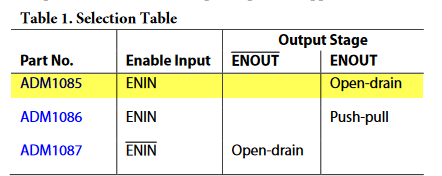
Respectively, the output pin ENOUT is required to have a pull-up resistor to 3V3 to properly support the #RST pin.
-
mon2
- XCore Legend
- Posts: 1913
- Joined: Thu Jun 10, 2010 11:43 am
Also double-check the wiring of your 3V3 voltage supervisor IC35 (STM1061) which does not appear to match the ST datasheet:
http://www.st.com/content/ccc/resource/ ... 065467.pdf
http://www.st.com/content/ccc/resource/ ... 065467.pdf
-
henkVerified
- Respected Member
- Posts: 347
- Joined: Wed Jan 27, 2016 5:21 pm
Kumar - excellent spot on the pin-out.
The design seems a wee-bit optimistic on the reset levels; 2.8V for 3V3 and 0.834 for 1V (my maths may be wrong).
You may want to put the scope on RST_N, 3V3 and 1V0; just to make sure the ordering is as expected?
Cheers,
Henk
The design seems a wee-bit optimistic on the reset levels; 2.8V for 3V3 and 0.834 for 1V (my maths may be wrong).
You may want to put the scope on RST_N, 3V3 and 1V0; just to make sure the ordering is as expected?
Cheers,
Henk
-
wlodek
- Member++
- Posts: 22
- Joined: Fri Jul 22, 2016 3:19 pm
Hi mon2,
Reset on the XHRA has a pull up I think but I will recheck.
As for the ST1061 - this seems to be wrongly wired !
Reset on the XHRA has a pull up I think but I will recheck.
As for the ST1061 - this seems to be wrongly wired !