Once-over before sending off the PCB ?

XCore Project reviews, ideas, videos and proposals.
SpacedCowboy
Experienced Member
Posts: 67
Joined: Fri Aug 24, 2012 9:37 pm

Once-over before sending off the PCB ?

Post by SpacedCowboy »

Hi guys,

So this is the first XMOS chip circuit I've "designed" (ie: heavily cribbed from other designs and stuffed together in a manner that might even work). I'm well aware of my limitations as a PCB designer (more of a software guy :), so if anyone would be good enough to give this a once-over and make sure I'm not doing anything *too* egregious, I'd really appreciate it.

The goal is to take a parallel-bus (at a relatively low frequency), serialise it to reduce the wire-count, and send changes over an xconnect link via cat-6 RJ45. That second XMOS chip will de-serialise the bus data and present it to clients as if they were connected directly to the original parallel bus. I won't go into more detail on the second chip and returned data because the circuit here is just the host-side.

In addition, the host side XMOS gets to expand the RAM of the host computer, by taking over the parallel bus and exposing its SDRAM in banks of mapped memory, and it provides a "hard drive" via an SD-card.


With that said, here's the schematic pages:

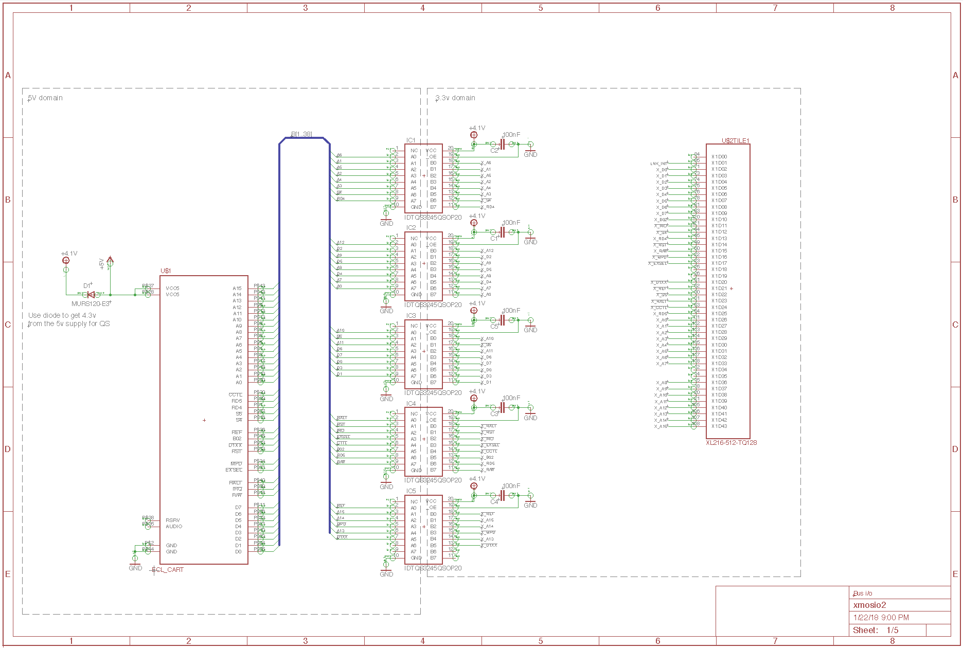
1: The host<==>XMOS parallel bridge
Image

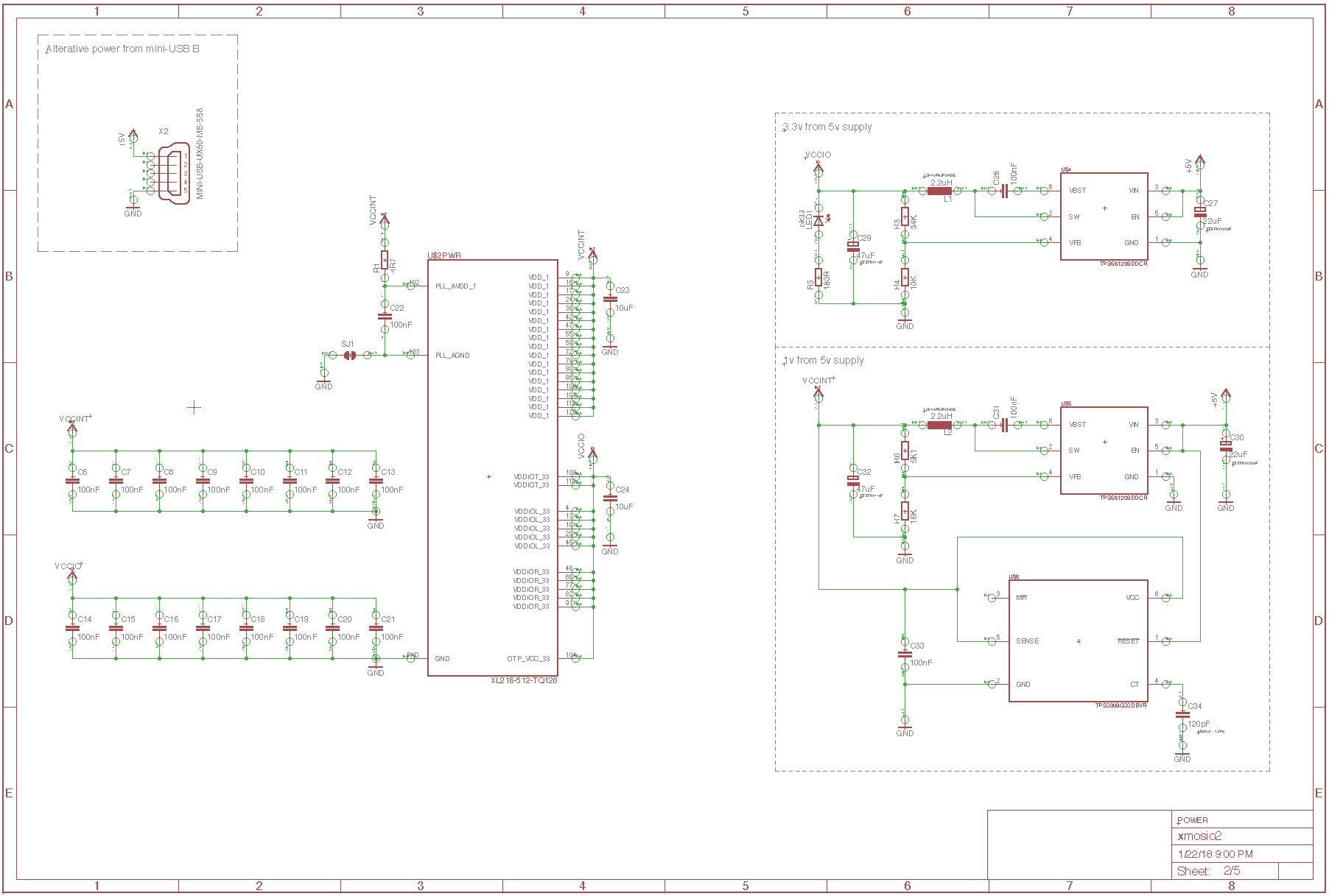
2: The power sequencing and voltage lines
Image

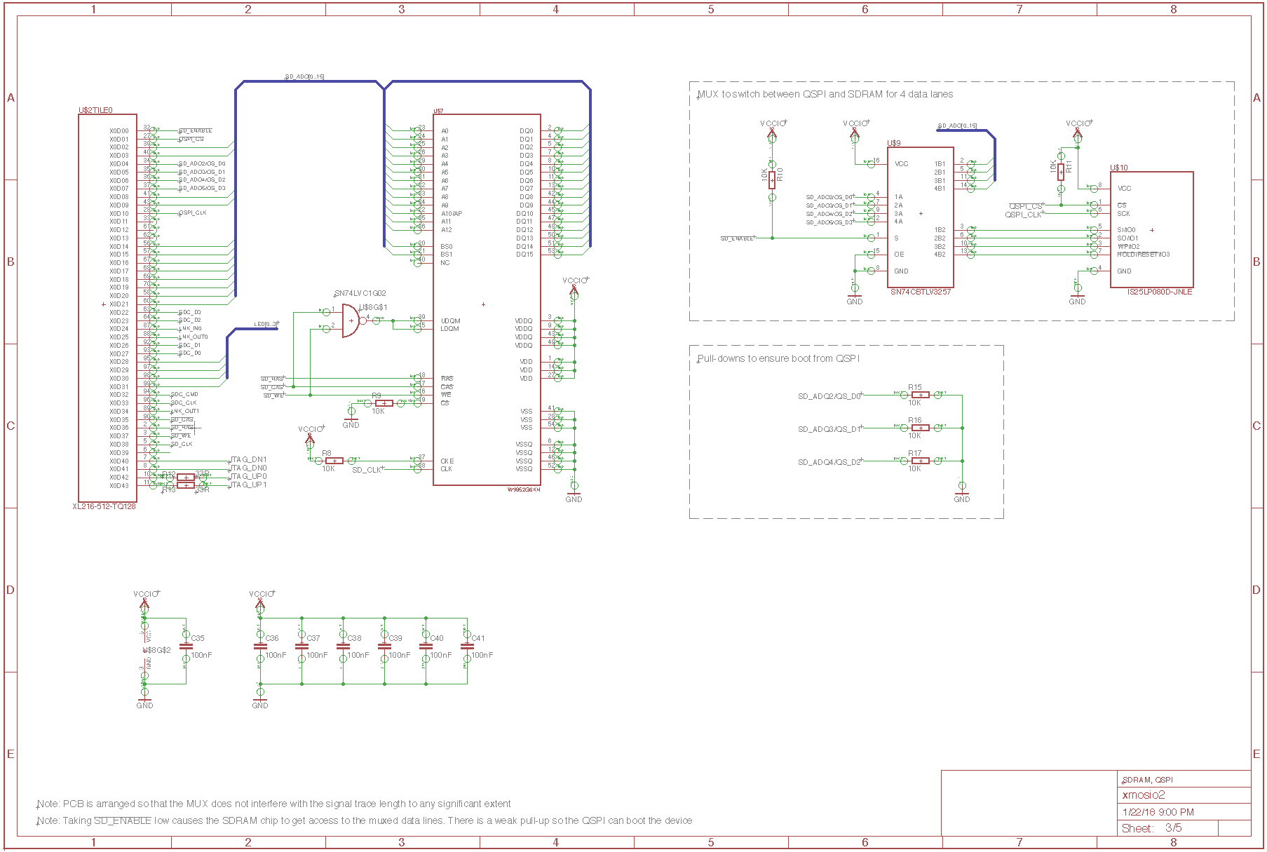
3: External memory (QSPI for boot, SDRAM for memory expansion)
Image

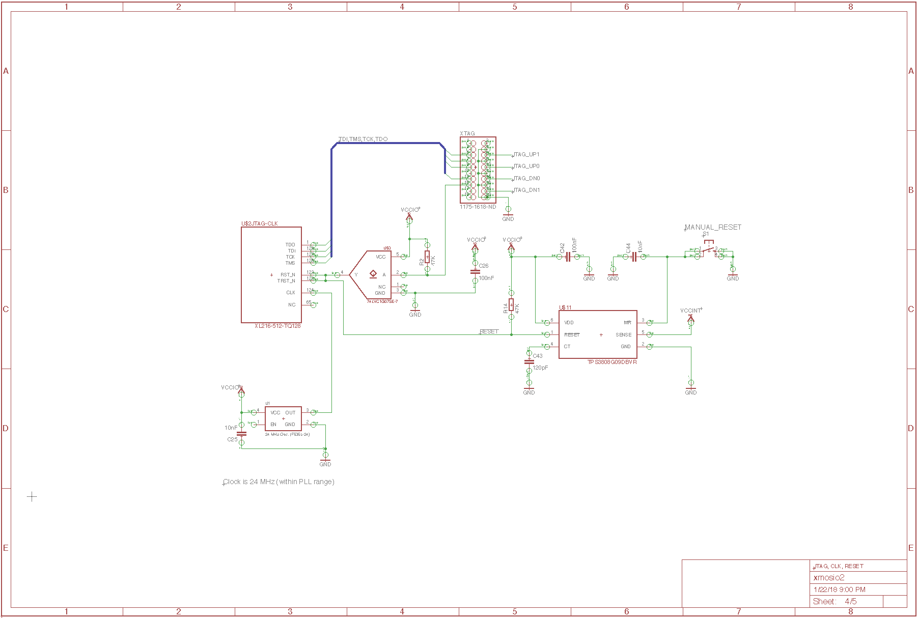
4: Clock and JTAG connection:
Image

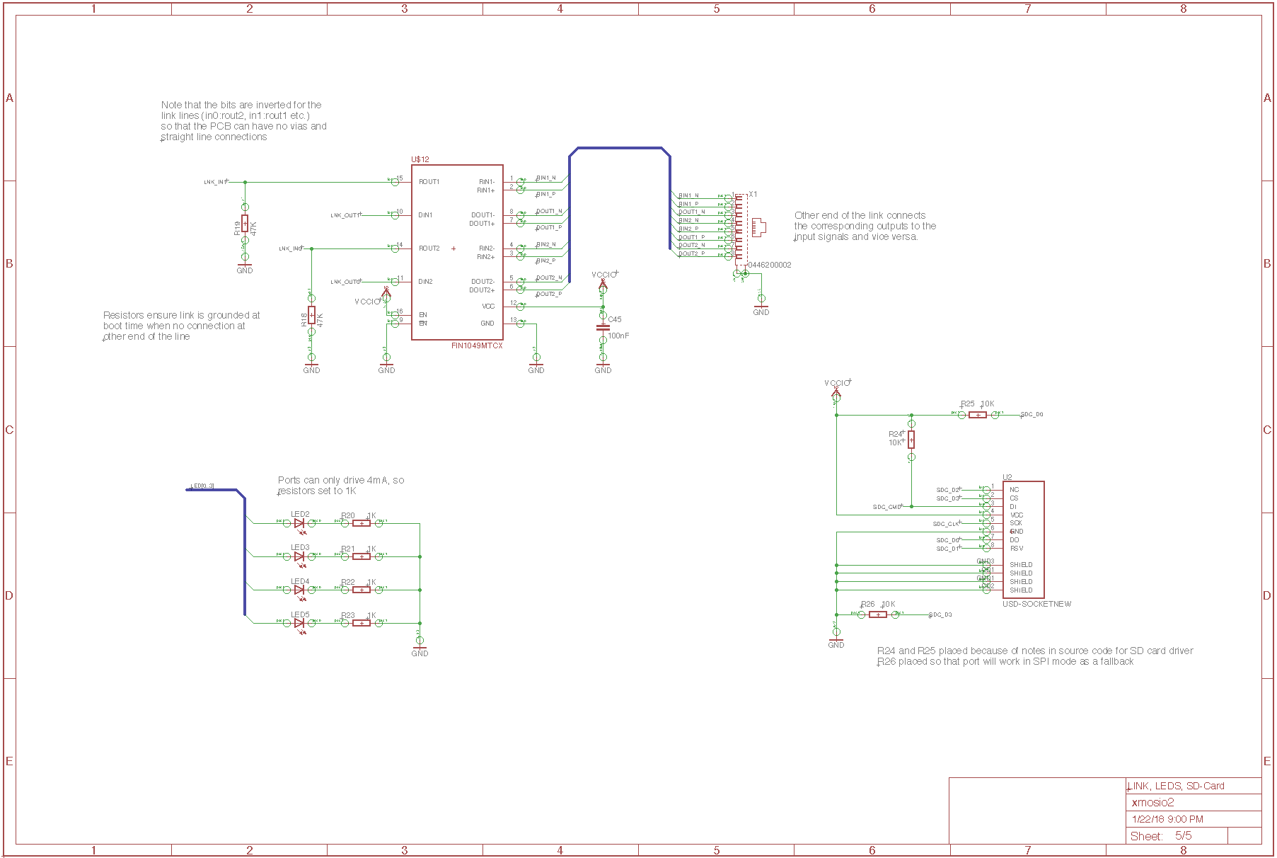
5: Link off-board, LEDs and 4-bit SD-card interface
Image

In addition, here's the PDF of the above, for easier viewing.

Questions I'm particularly interested in getting answers to
  • You can see in schematic 1/5 that the host side is 5v logic, and I'm using quick-switches to switch the logic level down to a more palatable 3.3v. I'm using a diode to convert the 5v down to 4.3v because I think there's a 1v drop within the quick-switch, which gives me a final voltage of 3.3v - can anyone who's done this confirm this actually works ? I really don't want to blow up the XMOS chip at power-on...
  • I'm also a bit nervous about the power-supplies. I've taken this from this project so I'm hopeful it'll work, but if anything jumps out at anyone, I'm all ears :)
  • On a general note, I've been using 10k for pull-down/pull-ups, for example on sheet 3/5 where the XMOS is set to boot from QSPI because X0D0{4,5,6} are all pulled low with a 10k pull-down. Is that an ok value ? Not too weak ?
  • I haven't attached a UART to the design because I'm hoping to use the XDebug interface on the XTAG connection. I'm using a 2-bit X0L0 link with 33R resistors on the drivers (out signals). On the PCB, these (together with the Link->differential-driver->RJ45) are the first-routed wires, are length-matched, have no vias and run over the ground plane. Is there anything else I ought to be looking out for ?
  • On sheet 5, the SD-card interface is laid out. The source for the SD-card 4-bit driver mentions that SDC_CMD and SDC_D0 ought to have pull-ups. The same question regarding suitability of the 10K applies here.
  • I'm also hoping to be able to fall-back to the 1-bit SPI mode, in which SDC_D3 operates as a /CS signal. I've put a weak pull down (again, 10K) to GND on that line. Is that likely to impact the 4-bit mode too much ? ie: Am I trying to have my cake and eat it here ?
Thanks for just reading this far :) If you could make any comments (especially if I've done something stupid) I'd really appreciate it. I'd like to keep the number of revisions of the board down if I can... 4-layer boards aren't cheap, and neither are all the components...

Cheers
Simon
User avatar
eez-open
Active Member
Posts: 60
Joined: Mon Oct 23, 2017 1:49 pm
Location: Croatia

Post by eez-open »

Schematics should be even more easier for viewing if you deselect layer 93 (Pins) :). You are missing pull-up resistor on U6 reset output (just as I did in my first version. The updated one can be found here (together with adjusted pads sizes on the PCB checked against real parts). Additionally, enable input from U6 is not wired correctly. It has to be connected to +3.3 V output not +1 V that you would like to control.
I don't understand how you came to conclusion that quickswitch will shift-down input voltages from 4.1 to 3.3 V. Why not simply use +3.3 V to power B-side? I can warmly recommend another 8-bit level-shifter if your budget allow that: SN74LVCC3245A. It support translation between many levels and comes in various packages (e.g. you can choose between SOIC and (T)SSOP depending of your soldering skills).
User avatar
eez-open
Active Member
Posts: 60
Joined: Mon Oct 23, 2017 1:49 pm
Location: Croatia

Post by eez-open »

SpacedCowboy wrote: On a general note, I've been using 10k for pull-down/pull-ups, for example on sheet 3/5 where the XMOS is set to boot from QSPI because X0D0{4,5,6} are all pulled low with a 10k pull-down. Is that an ok value ? Not too weak ?
If I understand datasheet correctly all pins are set low after reset. Therefore you don't need Pull-downs to ensure boot from QSPI section (Sheet 3/5). I cannot find it on XMOS' evaluation boards either (e.g. eXplorerKIT). QSPI_CS pull-up should remain. I've placed 10K on it too, it's possibly too weak if we compare it with 1K on eXplorerKIT, but that shouldn't be a problem to change once you allocate place for it on the PCB.
SpacedCowboy
Experienced Member
Posts: 67
Joined: Fri Aug 24, 2012 9:37 pm

Post by SpacedCowboy »

First off - thanks a lot for looking this over - I really do appreciate it :)
Schematics should be even more easier for viewing if you deselect layer 93 (Pins)
Duly noted - I thought I was doing pretty well to get rid of the grid [grin]

Code: Select all

 You are missing pull-up resistor on U6 reset output (just as I did in my first version. The updated one can be found here (together with adjusted pads sizes on the PCB checked against real parts). Additionally, enable input from U6 is not wired correctly. It has to be connected to +3.3 V output not +1 V 
Wow! Thanks - there was quite a lot wrong with that section! U5 had EN and Vin tied together as well! I think I must have copied/pasted it from the 3.3v converter and missed the differences. Thanks!
I don't understand how you came to conclusion that quickswitch will shift-down input voltages from 4.1 to 3.3 V
I may be misreading it, then, but I read the application note from IDT, and it says under 'Vout vs. Vin characteristics': "The QuickSwitch provides a low resistance connection between the input and output over a wide input voltage range. Starting from VIN of approximately –0.5V, the output voltage equals the input voltage. This relationship is maintained until the input voltage reaches approximately VCC –1V. For input voltages between VCC –1 and VCC, the output voltage gets clipped to approximately VCC –1 due to the ‘source-follower’ configuration of the N-channel switch". The SN74LVCC3245APWR do appear to be easier to use, but they're twice the price. I think for a first revision, everything else being equal, simpler is worth it, so I'll probably swap them out - thanks again :)
If I understand datasheet correctly all pins are set low after reset. Therefore you don't need Pull-downs to ensure boot from QSPI section (Sheet 3/5). I cannot find it on XMOS' evaluation boards
Yeah, I guess I can't see it on any of their docs either, so I can probably get rid of those.


Thanks again for input :)

Simon
SpacedCowboy
Experienced Member
Posts: 67
Joined: Fri Aug 24, 2012 9:37 pm

Post by SpacedCowboy »

So the latest version is now on github and here's a direct link to the PDF file for ease of browsing.

I've taken on-board eez-open's comments, and also added a few things:
  • Rename the power line from 4.1 to 4.3v. It was always *actually* 4.3v, it was just labelled as 4.1v
  • Make +5v be the only one with a specified width to aid in routing. The PCB traces are sufficiently wide, given they’re in air, and there are multiple supplies to the main chip
  • Added the required vias on the ground pad of the XMOS chip
  • Make LEDs be 0805 rather than 0603
  • Fixes identified by eez-open
  • Fix connection of 1v converter EN to +5V
  • Route JTAG lines and make Link lines pass DRC
  • Add LEDs for debugging later
  • Add a switch so that firmware can be booted from a golden master, rather than the latest on-board
I've decided to keep the quick switches because there's no need to set directionality with them. I do have a couple more areas I'd really like some input on though:
  • Do I need the 33R resistors on the external link ? I was reading the XMOS app-note on expected link performance and it seems to suggest that the 33R resistors are only needed in the absence of a real line-driver. Since I have a line-driver, anyone know if I need the resistors ?
  • The reset circuitry on sheet 4/5 has no pull-up on the /MR line. Does the capacitor do a similar job, or would I be better with a pull-up to VCCIO ?
Cheers
Simon
User avatar
mon2
XCore Legend
Posts: 1913
Joined: Thu Jun 10, 2010 11:43 am

Post by mon2 »

Hello Simon. Not agreeing with the use of the level shifter as shown in your schematic. To summarize, you wish to safely down shift the 5 volt signals to 3v3 for the XMOS and vice versa?

For a proper shifting, a dual voltage level translator is required. Recommend to review the following device from TI:

http://www.ti.com/lit/ds/symlink/txs0108e.pdf

Do note that one side is strictly for the lower Vcc rail while the other is respectively for the higher voltage rail (ie. 5v0). All such designs without directional control are FET based so have very wimpy drive capability. Do not attempt to use this translator with long cables and ideally use only for PCB based voltage translation. The way you are noting in your current design, the Vcc is @ 4v3 which is still very risky to use against the XMOS CPU. If anything, you could attempt to drive your choice of translator @ 3v3 and then the level shifting will be 5 volts down to 3v3 and XMOS 3v3 will output to 3v3 which may be enough for the 5 volt circuit to accept as a logic high. That is, with a single voltage supply, the translator is considered to be 5 volt tolerant but only will ever support 3v3 as a max. Please review the respective datasheet before proceeding but recommending the use of dual voltage translators.

Also saw the project is for the Atari use. OMG - old memories as I was to work @ Atari many moons ago. Recall meeting the Tramiel family (formerly founders of Commodore and then took over Atari); met Steve Wozniak; CEO of Batteries Included; actually ran into the author of Paperclip word processor a few times - Daniel Moore if I recall correctly @ Diamond Multimedia and then at another firm - believe he went to PLX Semiconductor later on. Small world. Learned so much on interfacing with hardware with our Atari fleet of computers in my teenage years + Rodnay Zaks 6502 programming. Priceless.

We have many recommendations for low cost PCB shops in Shenzhen if you are interested. Met some new ones during recent travels last October with excellent results.
SpacedCowboy
Experienced Member
Posts: 67
Joined: Fri Aug 24, 2012 9:37 pm

Post by SpacedCowboy »

To summarize, you wish to safely down shift the 5 volt signals to 3v3 for the XMOS and vice versa?
Yep, that's the plan. The XL/XE are 5v machines (what can I say, they're the machines of my heart from my dim and distant youth [grin]). I'm planning on implementing something like this. It turns out a 2-way link doesn't quite have the bandwidth for serializing the bus ... [th][td]5ns[/td][td]7.5ns[/td][/th]
Bandwidth, 2w (MB/s)1812
Time per byte (ns)5279
Pkt: send address data (bytes)55
Time for packet (ns)260395
Pkt: data-response (bytes)44
Time for packet208316
Time available for read op (ns)486-177 = 309309
Read op turnaround time (ns)309-208-260=-159-402
This is based on the timings:
Image

where the time from the address becoming valid and the machine potentially reading the D[7:0] lines is 309ns. On-chip, that's a non-issue, the SDRAM can be accessed and the value returned easily in that timeframe. Sending the bus-data (even if I strip it down to the minimal {command, 2-bytes for the bus, 2 bytes packet overhead} structure, it still takes 260ns at a 5ns beat time (which to be honest seems optimistic given that its going over RJ45). Add in the 208ns to return the data and I'm already out of time, even without any processing overhead.

... so I'll have to do it as a command/response expansion with a mailbox-type architecture, and copy the driver code from the device into the local SDRAM as part of boot up - that way the accesses are generally local and anything that really requires a round-trip can use the mailboxes. Since the device gets to specify its own driver, it can take appropriate steps to make sure it can handle the requests it needs to. I would have liked to just transport the parallel bus over the xconnect network and have the clients on the far side not be any different to a normal plug-into-the-machine interface, but I'll take what I can get. Moving to a 5-way link would solve my latency/bandwidth problems, but then I'd need 3 RJ45 connectors - at that point it starts to go from looking elegant to looking clunky. I might as well just put some line-drivers on and plug in a round IDE-bus cable...

This'll work because the time taken to do the ST{A,X,Y} of the address into the mailbox on the host XMOS is 4 cycles minimum, so by the time the 6502 gets around to reading the response to it's just-executed STA, the bus has had plenty of time to send the data, process it at the client end, and return a result. All of this can appear as mailbox addresses with a FETCH address and a PUT address for (respectively) read and write ops.

aaanyhoo - back onto topic, regarding your comments...

The quick-switches are designed to be level-converters, and the only reason I'm using 4.3v rather than 3.3 is the application note from their manufacturer - to quote: "The QuickSwitch provides a low resistance connection between the input and output over a wide input voltage range. Starting from VIN of approximately –0.5V, the output voltage equals the input voltage. This relationship is maintained until the input voltage reaches approximately VCC –1V. For input voltages between VCC –1 and VCC, the output voltage gets clipped to approximately VCC –1 due to the ‘source-follower’ configuration of the N-channel switch".

I was reading that as saying that if I set VCC to 4.3v, then the maximum value the QS will transmit on the low (nominally 3.3v) side is 3.3v. The paragraph on page 2 of that app-note says "The voltage drop across the switch when VIN = VCC is substantially constant for a wide range of supply voltage. The "clipping" action at high input voltages and the negligible voltage drop across the switch at lower input voltages makes the QuickSwitch an ideal device for voltage level translation in mixed 5V/ 3.3V systems. By using the QuickSwitch at a supply voltage of approximately 4.3V between a 5V bus and a 3.3 Volt bus, 3.3V signals can be passed to the 5V side without attenuation, and 5V signals will be clipped to 3.3V to interface safely with 3.3V circuits connected to the bus."

The 4.3v supply would in fact be only used on-PCB, I have a separate 3.3v supply (marked as VCCIO on all the schematics, derived from the 5v coming from the XL/XE) which drives all the on-board 3.3v logic. The 4.3v is purely for the supply to the quickswitches themselves, and only because of that application-note and the VCC-1 effect.

Having said all that, I've now got 2 votes against! I'm losing faith in my comprehension abilities :)

PS: Kind of cool you working at Atari - I'll bet you have a fair number of interesting memories about that place :) It was the machine I first cut my teeth on, it came with a disk drive (as opposed to the tape deck of my previous computer, the Sinclair ZX81, and it had the first genuine separate video subsystem, which blew my mind :) It started me out on programming, and here I am, 40 years later, working on hardware, firmware, and software in R&D at Apple, living 6000 miles away from where I was born. I sometimes wonder how different my life would have been if I hadn't pleaded and pleaded for that machine for Xmas, and then actually been given it...

Cheers
Simon
SpacedCowboy
Experienced Member
Posts: 67
Joined: Fri Aug 24, 2012 9:37 pm

Post by SpacedCowboy »

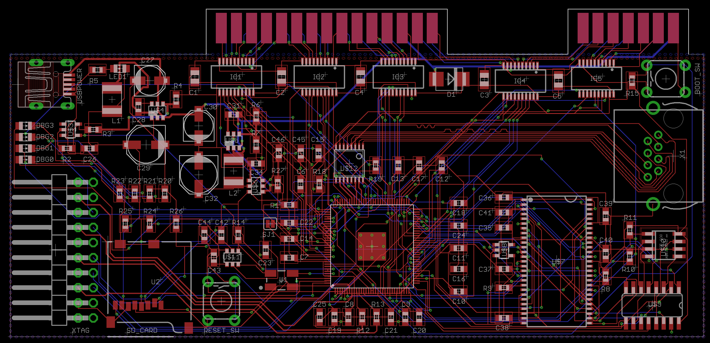
So assuming my conclusions about the Quickswitches are in fact ok, I went ahead and routed the board out - here it is displayed without the inner layer VCCIO and GND polygon pours, for clarity...
Image
Some thoughts.
  • XTAG is freaking huge.
  • You can see the LVDS bus towards the top-left U$12 -> X1. The lines are length-matched (see below) to a reasonable level
  • Less obvious are the JTAG link lines (left-most row of the XTAG, 3rd, 5th, 7th, and 9th up from the bottom) - again these are length-matched within their groups (receive, transmit)
  • SDR SDRAM length-matching isn't as critical as DDR, but these are all within reasonable tolerances of each other. I was watching out for CLK being radically different from any of the ADQ lines
There's a neat ULP in Eagle to tell you more than you wanted to know about your traces - open up the board and type 'run length-freq-ri' into the command at the top. I got:

Code: Select all

Signal	f max. [MHz]	l [mm]	A [mm2]	R [mOhm]	w min [mm]	w max [mm]	Imax [A]

RIN1_N	   4452.19	 67.338	0.004	 263.59	 0.127	 0.127	  0.42
RIN1_P	   4457.12	 67.263	0.004	 263.30	 0.127	 0.127	  0.42
RIN2_P	   4621.87	 64.865	0.004	 253.92	 0.127	 0.127	  0.42
RIN2_N	   4657.59	 64.368	0.004	 251.97	 0.127	 0.127	  0.42

DOUT2_N	   5005.61	 59.893	0.004	 234.45	 0.127	 0.127	  0.42
DOUT2_P	   5056.56	 59.289	0.004	 232.09	 0.127	 0.127	  0.42
DOUT1_N	   5096.74	 58.822	0.004	 230.26	 0.127	 0.127	  0.42
DOUT1_P	   5101.53	 58.767	0.004	 230.04	 0.127	 0.127	  0.42

JTAG_DN1	   5130.91	58.430	0.007	 142.95	 0.203	 0.203	  0.65
JTAG_DN0	   5235.62	57.262	0.007	 140.09	 0.203	 0.203	  0.65
JTAG_UP1	   5412.80	 55.387	0.007	 135.51	 0.203	 0.203	  0.65
JTAG_UP0	   5513.79	 54.373	0.007	 133.03	 0.203	 0.203	  0.65
Which I was reasonably happy with. The SDRAM figures weren't quite as good (I left the autorouter to do the job) but they're within reason. Max length difference from CLK is about 15mm.

Oh, and if anyone has any insight, I'd still like to know:
  • Do I need the 33R resistors on the external link ? I was reading the XMOS app-note on expected link performance and it seems to suggest that the 33R resistors are only needed in the absence of a real line-driver. Since I have a line-driver, anyone know if I need the resistors ? Currently I have none. Thinking about putting in the pads and not stuffing the parts...
  • The reset circuitry on sheet 4/5 has no pull-up on the /MR line. Does the capacitor do a similar job, or would I be better with a pull-up to VCCIO ?
User avatar
eez-open
Active Member
Posts: 60
Joined: Mon Oct 23, 2017 1:49 pm
Location: Croatia

Post by eez-open »

SpacedCowboy wrote: Do I need the 33R resistors on the external link ? I was reading the XMOS app-note on expected link performance and it seems to suggest that the 33R resistors are only needed in the absence of a real line-driver. Since I have a line-driver, anyone know if I need the resistors ? Currently I have none. Thinking about putting in the pads and not stuffing the parts...
Maybe to be on the safe side, allocate places for resistors that you can solder 33R or just 0R.
SpacedCowboy wrote: The reset circuitry on sheet 4/5 has no pull-up on the /MR line. Does the capacitor do a similar job, or would I be better with a pull-up to VCCIO ?
I'd like to suggest a pull-up that is already there (R14).

Apart from that, possibly that I'm not interpreting your PCB layout correctly, but I can find dozens of overlapping between traces on "red" layer! Did you run error checking?
Also decoupling capacitors could be in smaller proximity from MCU power pins.
SpacedCowboy
Experienced Member
Posts: 67
Joined: Fri Aug 24, 2012 9:37 pm

Post by SpacedCowboy »

I think you're right about the 33R - that's a better way of saying what I was trying to articulate :)

R14 is on /RESET, not on /MR. I was thinking that the manual reset button ought to be pulled up, so that there's a guaranteed transition when you ground it by pressing the button.

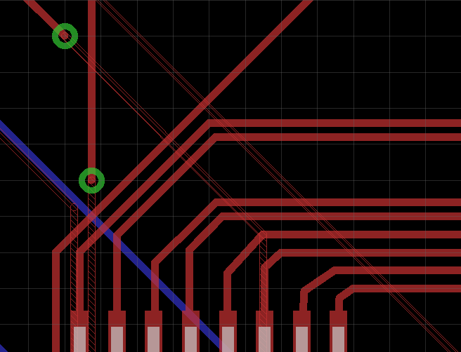
There are 4 layers on the board - one of which is shown with a hatched-red drawing style. If I run DRC, I get 9 errors, all of which are "overlap"-type, and are caused by the vias within the central pad of the XMOS chip, which I expect. Actually looking at the image, it's really not clear. I really wish they'd used a different colour before going to a hatched patter of an existing colour. Seems to me there's a lot more colours than red and blue...

Zooming in gets you something that looks like:
Image
I'd like to get the decoupling caps closer, but routing starts to get harder the closer they are. I may try pulling them in a bit and see how far I can get it before breakage.

Thanks again for the comments :)

Simon